You have that sinking feeling when you are about to start up your high-speed PCB, the first time. Will those specially laid differential pairs work? Are your impedances correct? Did you take into consideration that stubborn crosstalk between traces? The long-held notion has been to set it to lab and find out, but what if you are not privy to the renowned multimillion dollars of oscilloscopes and vector network analyzers?
The good news is that you can actually predict and verify signal integrity problems, before you have even left the fabrication house with your board. Nothing can substitute real measurements, but nowadays, with the help of potent simulation tools and calculation techniques, modern designers can discover the majority of the issues at the initial stages.
Discovering What Really Matters
We should get an idea of what we are actually checking before going into tools and techniques. Signal integrity is not some kind of magic that can only manifest itself in the lab. It is all about ensuring that you have proper impedance in all of your signal path, reducing reflections that distort your data and ensuring that signals do not interfere.
The beauty of it is that the three can be mathematically forecasted. These characteristics are defined long before an electron ever flows by your PCB stackup, trace geometries, and material properties. This ensures that you are able to detect problems at the design phase instead of doing a board respin at a high cost.
Begin With Impedance Control
Signal integrity is based upon impedance matching, particularly when the frequency of operation is above a few megahertz. The misalignment of this ensures that there are reflections, ringing and even inoperable circuits. The old way is to do a lot of calculations, depending on your PCB stackup, but it has a much simpler point of departure.
PCB impedance calculator online will save you hours of tedious calculations and provide you with instant feedback on the geometry of your traces. These calculators input your stackup parameters; dielectric height, copper thickness, dielectric constant and give you the exact trace dimensions you should use to achieve your desired target impedance. The trick is not to use them once but use them over and over again in the designing process.
The value of such calculators is that they make you realize the trade-offs. Require 50 ohms but your traces are too wide? It is easy to understand the effect of varying your dielectric height or swapping to an alternate layer on your choice.
Getting Your Geometry Right

After having your target impedance, the next thing you are faced with is to implement it uniformly on your board. Here is where PCB trace width is important and it is not simply about choosing a number and rolling on. Various parts of your board may not have the same stackup and manufacturing tolerances imply that your trace width may not be the same as nominal.
The intelligent solution is to design marginally. You may have to get 6 mils to make 50 ohms, but know that production variations may change your figure to 5.5 to 6.5 mils. Test your impedance over that range. The vast majority of fabricators are capable of holding +/-0.5 mils on trace width, although the understanding of how it impacts your impedance will guide you on where you want to be conservative.
Trace length matching is also another aspect that is usually ignored. Even perfect control of impedance is not going to help you if your traces are of radically different lengths in case of differential pairs or parallel buses. Contemporary EDA tools have the ability to indicate lengths mismatches in real-time, and measurements can be employed to forecast timing skew even prior to hardware construction.
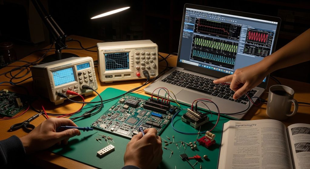
Simulation Is Your Secret Weapon
Here lies the point of great interest. Free and low-cost circuit simulators are now very elaborate. You are able to simulate your whole signal path, including driver and traces, vias, connectors, receiver and see precisely what your eye diagram will be like or where reflections are going to be.
Simulators based on SPICE allow you to add IBIS models of your drivers and receivers (typically provided at no cost by chip vendors) and S-parameter models of your connectors. Then you pour in transmission line models using the calculated impedances and, all of a sudden, you are starting to observe signal behavior, which could previously only be observed using very expensive lab equipment.
It is a trick to begin simple and only add complexity where it is necessary. Start with a simple trace-receiver-driver model, check that it is sensible, and then introduce parasitances, crosstalk from adjacent traces, and via discontinuities.
Don’t Forget About Power Integrity
Power integrity and signal integrity go hand in hand particularly at high speeds. An ideal 50 ohm trace does not assist when your power delivery system is incapable of providing clean and stable voltage when your circuits require it. Similar simulation techniques can be used to model your PDN, and you can check impedance versus frequency and find resonances. Power delivery impedances are generally significantly less, usually less than an ohm, yet the same principles still apply.
Practical Validation Steps
In addition to simulation, some free practical sanity checks can be used to detect the usual errors. Determine your signal rise times and compare them with your trace lengths. When your rise time is greater than twice your propagation delay transmission line effects are unlikely to dominate. This is a test that can be run quite easily and will tell you whether you need to bother with controlled impedance on a given set of nets at all.
Check your currents in your returns. Any high-speed signal requires a low-impedance return path, and cuts on your ground plane can have a disastrous effect. These problems are visible in your layout tool, you do not need lab equipment.
Beyond the Board
Although we have concentrated on PCB design, the issues of signal integrity are also applied to the connection of the boards to each other, as well as the connection of the boards to the world. The Custom wire harness manufacturing has a lot of the same considerations–impedance control, noise immunity, and a good signal transmission–only in a different physical format. Once you start transitioning to board-level traces into individual wires, an online wire size calculator will come in handy to make sure your interconnects do not become the weak point in your system.
Moving Forward With Confidence
Signal integrity can be achieved without using costly laboratory tools, and the first step is not corner cutting. It is about using the strong prediction and simulation tools currently in the possession of all designers. With careful modeling and computation before fabrication, you will be able to obtain reliable high-performance designs and save the time you would have devoted to oscilloscope time-wasting problem-hunting instead of validating the design.