Introduction
In today’s electronics world, the push for smaller, faster, and more capable devices means that manufacturing teams face new challenges. One of those challenges is working with assemblies that use a high density of components, especially the specialized packages known as ball grid arrays (BGAs). When you combine that packaging with very tight spacing between solder balls, you end up with what we call fine‑pitch BGA PCB assembly. Because the spacing is so small and the tolerances so tight, inspection and rework of these assemblies must be handled carefully to maintain quality, reliability, and performance.
This article takes a deep dive into inspection and rework strategies specifically for fine‑pitch BGA assemblies. Whether you’re a PCB designer, assembly engineer, or quality control specialist at a facility like FastTurnPCBs fastturnpcbs, you’ll find useful guidance. We’ll cover key inspection techniques, common defects, tools and methods for rework, and strategies to boost yield and reliability.
Understanding Fine‑Pitch BGA PCB Assembly
To begin, it’s helpful to know what we mean by fine‑pitch BGA PCB assembly and why it poses special inspection and rework challenges. Fine‑pitch refers to the center‑to‑center spacing of the solder balls or pads under the BGA package. According to industry sources, fine‑pitch may mean pad or ball spacing of 0.5 mm or less, or in ultra‑fine cases even 0.35 mm or lower. The tighter the spacing, the more difficult it is to route signals, design vias, and manufacture reliable solder joints.
In fine‑pitch BGA PCB assembly, the small pad size, high pad count, and limited escape routes make both assembly and inspection more demanding. For example, one guide notes that when you get into 0.5 mm or lower ball pitch, standard through‑hole vias may not work and you may need microvias or via‑in‑pad to escape signals from beneath the BGA. Because the solder balls are hidden beneath the package, visual inspection is typically not enough; advanced techniques like X‑ray or acoustic microscopy often become necessary. Thus, for companies that offer fine‑pitch BGA PCB assembly services—such as FastTurnPCBs—planning inspection and rework strategies early is critical to ensure quality outcomes.
Key Inspection Methods for Fine‑Pitch BGA Assemblies
When working with fine‑pitch BGA boards, inspection techniques must step up from standard methods. One primary method is X‑ray inspection. Because the solder joints of a BGA package are hidden beneath the package body, X‑ray allows you to see voids, cold joints, misalignment, bridging, and solder ball failures. Industry commentary explains that as ball pitch shrinks, inspection becomes more complex and mandatory: “Fine‑pitch BGAs need advanced PCB fabrication and precise SMT assembly… X‑ray inspection is mandatory.”
Another important inspection method is solder‑paste inspection (SPI) and automated optical inspection (AOI) of stencil print and placement prior to reflow. For fine‑pitch assemblies, ensuring that solder paste deposition is uniform, correctly aligned, and free of defects like insufficient volume or bridging is critical. For example, one guideline shows that for a 0.5 mm pitch BGA, the stencil design must take into account area ratio and aperture geometry. Additionally, after reflow, voiding or ball mis‑alignment can severely impact reliability, so post‑reflow inspection must check for those issues.
When selecting inspection methods for a fine‑pitch BGA PCB assembly, you should also consider board warpage, BGA coplanarity, solder ball integrity, and package seating. The inspection strategy should include pre‑reflow checks (print, placement, ball seating), post‑reflow checks (X‑ray, AOI, functional test), and periodic monitoring of process key metrics (voiding percentage, ball attach yield, alignment offset). By integrating these inspection methods early, assembly operations at FastTurnPCBs or similar services can reduce failures and expedite rework when needed.
Common Defects and Their Causes in Fine‑Pitch BGA Assemblies
Even with best practices, fine‑pitch BGA assemblies are susceptible to a variety of defects due to their complexity. One common defect is solder ball misalignment or off‑centre placement under the BGA package. Because the pitch is tight, even small shifts during placement or reflow can result in open joints or bridging to adjacent balls. Another major defect is voiding within the solder joint. Voiding reduces joint cross‑section and can lead to thermal or mechanical failure over time. As design guides point out, voiding becomes more prevalent when pad design, stencil aperture, or reflow profile are not optimized.
Bridging or solder shorts between adjacent balls is also a higher risk in fine‑pitch BGA assemblies. With smaller spacing, solder paste deposition must be tightly controlled; any overprint or mis‑placement can create a bridge. Additionally, pad design or via fan‑out constraints can contribute to weak solder joints or pad cratering. For example, when routing beneath fine‑pitch BGAs, using via‑in‑pad or microvias may raise fabrication cost but helps avoid pad cratering and helps reliability. Other defects include tomb‑stoning of BGAs (if one side lifts during reflow), package warpage, and board warpage causing uneven solder ball compression. For inspection and rework strategies to be effective, these common defects must be well‑understood by the manufacturing and quality teams.
Rework Strategies for Fine‑Pitch BGA Assemblies
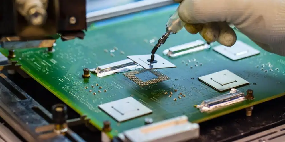
When a fine‑pitch BGA board fails inspection or functional testing, the rework strategy must be both precise and controlled to avoid damaging adjacent components. The first step is to localize the defect using inspection data — whether from X‑ray, AOI, or functional test logs — and determine if the problem is isolated to a particular BGA or is systemic across the board. If it’s isolated, removal of the BGA package is the next step.
Package removal requires specialized equipment: hot‑air or infrared rework stations with vacuum pick‑and‑place tooling, precise temperature profiles to prevent board damage, and sufficient control to avoid pad lifting or delamination. Because fine‑pitch BGA pads are small and tightly spaced, any damaged pad or lifted trace can render the site unusable. After removal, the site must be cleaned of residual solder, flux residue, and any damaged material around the pads or microvias.
Once prepared, the rework site must be verified for pad integrity, planarity, and cleanliness before placing the replacement BGA. Solder paste or pre‑reflowed ball attach should match the original specification—especially for fine‑pitch BGAs, where the ball pitch, pad geometry, and solder volume are critical. After placing the new package, a reflow profile matching the original assembly’s thermal profile should be used, with bubble‑free soldering and X‑ray post‑reflow inspection to confirm joint integrity. It is also a good practice to run a functional or stress test to confirm reliability.
Finally, when developing rework strategies for fine‑pitch BGA PCB assembly, it’s wise to build a rework evaluation protocol. This protocol may include checking for pad condition (visual, optical), verifying ball formation (X‑ray), measuring voiding or joint shape, and performing thermal cycling or mechanical stress testing if the assembly is intended for high‑reliability applications. A well‑defined rework strategy reduces downtime, waste, and risk — helping services like FastTurnPCBs maintain high reliability in fine‑pitch BGA boards.
Process Optimization and Best Practices for Yield Improvement
While inspection and rework are vital, optimizing the upstream process for fine‑pitch BGA PCB assembly is equally important for yield improvement. First, design for manufacturability (DFM) plays a key role. When a board is designed with tight ball pitch BGAs, the PCB design must support proper pad geometry, via fan‑out, solder mask definitions, and controlled impedance if required. One guide notes that via‑in‑pad or microvia escape routing becomes necessary once you go to 0.4 mm pitch BGAs. When FastTurnPCBs offers fine‑pitch BGA PCB assembly, collaborating with customers at the design stage to discuss these constraints significantly reduces downstream defects.
Second, stencil design and solder paste control are critical. For fine‑pitch BGA assemblies, the deposition of solder paste must ensure uniformity, repeatability, and the correct solder volume. For example, in 0.5 mm pitch BGA applications, stencil aperture geometry (such as circular vs square openings) influences solder paste transfer and subsequent joint quality. Third, pick‑and‑place equipment and reflow furnace capabilities must be verified to meet the precision requirements of fine‑pitch BGAs. The placing accuracy must align with the ball grid pattern, and thermal profile control must prevent warpage and promote reliable solder joints. Additionally, process monitoring of key metrics — such as alignment offset, voiding percentage, solder volume variation — can help identify and remedy issues early.
Lastly, continuous feedback from inspection and rework operations helps drive process improvement. When defects are tracked and traced to root causes (whether pad design, stencil issue, component placement, or reflow profile), the assembly facility can refine its process, update guidelines for fine pitch BGA PCB assembly, and reduce the need for rework. By combining DFM, precise assembly, tight inspection, and informed rework strategies, companies like FastTurnPCBs can deliver high‑quality fine‑pitch BGA assemblies with strong reliability and customer satisfaction.
Conclusion
In the highly demanding field of electronics manufacturing, fine‑pitch BGA PCB assembly represents one of the most intricate challenges. The combination of high ball count, tight spacing, limited escape routes, and hidden solder joints elevates inspection and rework requirements. For firms engaged in this kind of assembly — such as FastTurnPCBs — a structured approach that covers design collaboration, precise inspection (including X‑ray and SPI/AOI), dedicated rework strategies, and continuous process optimization is essential.
By understanding the common defects, employing appropriate inspection methods, establishing safe and effective rework protocols, and optimizing the upstream assembly process, manufacturing teams can achieve high yields, low defect rates, and reliable end products. For any project involving fine‑pitch BGAs, taking inspection and rework seriously is not just best practice — it is a necessity for delivering high‑performance electronics in today’s competitive market.