

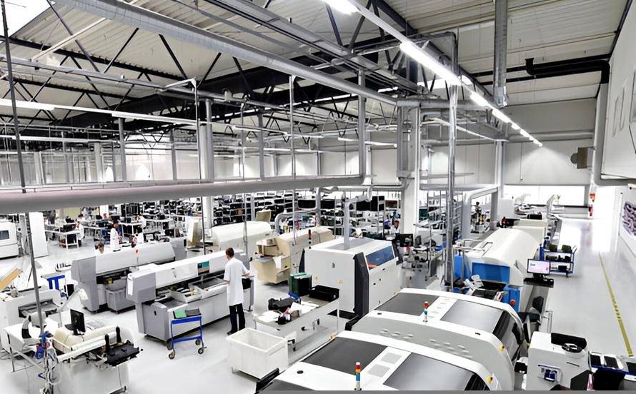
Printed circuit boards are the foundation of modern electronics, enabling everything from smartphones and medical devices to aerospace systems, automotive electronics, industrial automation, and telecommunications equipment. As electronic products become more compact and technologically advanced, the demand for precision-engineered circuit boards continues to increase. Producing these boards requires a highly controlled production workflow that ensures every electrical connection, copper trace, and drilled hole meets strict quality standards. This comprehensive workflow is known as the PCB Manufacturing Process.
The manufacturing process involves much more than transferring a circuit design onto a board. Every stage, from material selection and layer imaging to drilling, plating, surface finishing, and electrical testing, contributes to the performance and reliability of the finished PCB. Even minor manufacturing errors can affect signal integrity, thermal performance, or long-term product durability.
For industries that require strict quality compliance, many businesses partner with experienced PCB Manufacturers in the USA. American manufacturers are recognized for their engineering expertise, advanced manufacturing technologies, strong quality management systems, and compliance with demanding industry standards for aerospace, defense, medical, and industrial applications.
This article explains the PCB manufacturing process, discusses its importance, explores quality control practices, and examines why PCB manufacturers in the USA remain trusted partners for high-performance electronic products.
What Is the PCB Manufacturing Process?
The PCB Manufacturing Process is the series of engineering and production steps used to transform a digital circuit board design into a finished printed circuit board ready for electronic assembly. Each manufacturing stage requires high precision because modern circuit boards often contain thousands of electrical connections within extremely compact layouts.
The process begins after engineers complete the PCB design using electronic design automation software. Manufacturing files, including Gerber files, drill data, fabrication drawings, and layer stack-up information, are prepared for production.
Unlike simple mechanical products, printed circuit boards require precise control of electrical, thermal, and mechanical characteristics. Copper thickness, dielectric materials, hole positioning, conductor spacing, and layer alignment must all remain within extremely tight tolerances to ensure proper functionality.
Whether producing a simple two-layer PCB or a sophisticated high-density interconnect design, every manufacturing stage contributes directly to the reliability of the finished electronic product.
Design Verification Before Production
Before physical manufacturing begins, engineering teams perform an extensive review of the customer’s design files. This evaluation ensures the design can be manufactured efficiently while maintaining the required quality standards.
Design for Manufacturability (DFM) analysis identifies potential issues involving trace widths, spacing, via sizes, solder mask clearances, copper balancing, and board dimensions. Engineers may recommend design modifications that improve production yield without affecting electrical performance.
This early verification process significantly reduces manufacturing risks by identifying problems before production begins. It also helps minimize production delays, engineering revisions, and unnecessary manufacturing costs.
For highly complex products such as medical devices or aerospace electronics, design verification becomes an essential part of ensuring long-term product reliability.
Material Preparation and Layer Formation
Once the design has been approved, production begins with selecting the appropriate laminate materials. FR-4 remains the most commonly used substrate because of its excellent mechanical strength, electrical insulation, and cost-effectiveness. Specialized applications may require high-frequency laminates, ceramic materials, metal-core substrates, or polyimide materials depending on operating conditions.
Copper-clad laminate panels serve as the starting point for fabrication. Using advanced photolithography techniques, manufacturers transfer the circuit pattern onto the copper surface through a photosensitive coating.
After exposure and development, chemical etching removes unwanted copper, leaving only the required conductive traces that form the electrical circuitry. This process must be carefully controlled to maintain accurate conductor widths and spacing throughout the board.
For multilayer boards, internal layers are individually fabricated before being aligned and laminated into a single integrated structure.
Drilling, Plating, and Layer Interconnection
Once the circuit layers have been created, precision drilling equipment produces holes for electrical interconnections and component mounting. Modern manufacturing facilities utilize both mechanical drilling and laser drilling depending on the design requirements.
Laser drilling enables the creation of microvias required for High-Density Interconnect (HDI) circuit boards, while mechanical drilling remains suitable for conventional through-hole structures.
Following drilling, the holes undergo copper plating to establish reliable electrical connections between multiple circuit layers. Uniform copper deposition is essential because inconsistent plating may reduce electrical performance or long-term reliability.
For multilayer circuit boards, multiple lamination and plating cycles may be required to achieve the final board structure while maintaining precise layer alignment throughout the manufacturing process.
Surface Protection and Finishing
After the conductive circuitry has been completed, protective coatings are applied to improve durability and prepare the board for electronic assembly. A solder mask is deposited over the board surface to protect exposed copper from oxidation while preventing unintended solder bridges during component assembly.
Silkscreen markings are then printed to identify component locations, reference designators, polarity indicators, and assembly information. These markings assist technicians during assembly, inspection, and future maintenance.
The exposed copper pads receive a protective surface finish that ensures excellent solderability while protecting the copper from environmental degradation. Common finishes include Hot Air Solder Leveling (HASL), Electroless Nickel Immersion Gold (ENIG), Organic Solderability Preservative (OSP), immersion silver, and immersion tin.
The selection of surface finish depends on the intended assembly process, product requirements, and expected operating environment.
Inspection and Quality Control Throughout Manufacturing
Quality assurance plays a critical role throughout every stage of PCB manufacturing. Manufacturers continuously inspect the product to verify dimensional accuracy, electrical integrity, and compliance with customer specifications.
Automated Optical Inspection (AOI) systems compare fabricated circuit patterns against the original design data to identify defects such as missing traces, short circuits, incorrect conductor widths, or manufacturing inconsistencies.
Electrical testing verifies circuit continuity while ensuring no unintended electrical connections exist between conductive paths. Flying probe testing and bed-of-nails testing are commonly used depending on production volume and board complexity.
For multilayer and HDI designs, X-ray inspection evaluates hidden internal structures including plated vias and buried interconnections that cannot be inspected visually.
Many manufacturers also perform impedance verification, thermal stress testing, dimensional analysis, and reliability evaluations to ensure every circuit board meets required performance standards before shipment.
Why PCB Manufacturers in the USA Remain Highly Respected
Many companies choose PCB Manufacturers in the USA because of their strong commitment to engineering quality, advanced manufacturing capabilities, and regulatory compliance. American manufacturers have extensive experience producing highly reliable circuit boards for industries where product performance and safety are essential.
The aerospace and defense sectors depend heavily on domestic PCB production due to strict security requirements and demanding quality standards. Medical device manufacturers also value the rigorous manufacturing controls maintained by U.S. facilities, particularly for products requiring FDA compliance and long-term reliability.
American manufacturers invest heavily in advanced production technologies, including laser direct imaging, automated optical inspection, precision drilling equipment, intelligent manufacturing systems, and sophisticated quality management software.
Another important advantage is engineering collaboration. Close communication between customers and manufacturing teams often leads to faster design optimization, reduced production risks, and improved product performance throughout the development process.
Applications Requiring High-Quality PCB Manufacturing
The PCB manufacturing process supports nearly every technology-driven industry. Consumer electronics manufacturers rely on precision circuit boards for smartphones, laptops, wearable devices, and smart home products.
Automotive companies require reliable PCBs for electric vehicles, battery management systems, advanced driver assistance systems, infotainment platforms, and engine control electronics.
Medical equipment manufacturers utilize advanced circuit boards in diagnostic imaging systems, patient monitoring equipment, implantable devices, laboratory analyzers, and portable healthcare products.
Industrial automation systems, telecommunications infrastructure, robotics, renewable energy equipment, aerospace electronics, military systems, and artificial intelligence hardware also depend on precision PCB manufacturing to ensure reliable long-term performance.
As electronic technology continues to evolve, demand for sophisticated PCB manufacturing capabilities will continue to expand across every major industry.
Future Trends in PCB Manufacturing
The future of PCB manufacturing is being shaped by rapid advances in electronics design and manufacturing automation. Artificial intelligence, electric mobility, high-speed communication, wearable healthcare devices, and industrial digitalization require increasingly complex circuit board technologies.
Manufacturers are investing in smart factory automation, artificial intelligence-driven inspection systems, predictive process monitoring, laser direct imaging, additive manufacturing techniques, and environmentally sustainable production methods.
Emerging PCB technologies such as embedded components, ultra-high-density interconnects, advanced thermal management materials, and flexible hybrid electronics will further expand the capabilities of future electronic products.
As manufacturing precision continues to improve, PCB production will support increasingly sophisticated electronic systems while maintaining exceptional reliability and production efficiency.
Conclusion
The PCB Manufacturing Process is a highly engineered sequence of fabrication, inspection, and quality assurance procedures that transforms electronic designs into reliable printed circuit boards capable of supporting today’s advanced technologies. Every manufacturing stage, from material preparation and copper patterning to drilling, plating, surface finishing, and testing, contributes directly to product performance and long-term reliability.
Partnering with experienced PCB Manufacturers in the USA provides businesses with access to advanced engineering expertise, precision manufacturing technologies, strict quality control systems, and regulatory compliance required for demanding industries such as aerospace, medical, automotive, telecommunications, and industrial automation. As electronic products continue to become smaller, faster, and more intelligent, high-quality PCB manufacturing will remain the foundation of innovation across the global electronics industry.
