You have spent hours and hours creating your PCB, adjusting traces, assembling components, and executing design rule checks. Everything appears to be all right on your screen. However, prior to you clicking that send button to your manufacturer, one very important step between amateur designers and professional designers is to check your Gerber files well before you send them.
Imagine Gerber files as the common language between your design application and the factory. They are simply a series of instructions that command the fabrication equipment on where to etch copper, drill holes and solder mask. The slightest mistake in such files may result in expensive mistakes, delays in production, or boards that just do not work. The good news? You can prevent these problems before they turn out to be costly by using the appropriate strategy and tools.
Understanding What You’re Actually Looking At
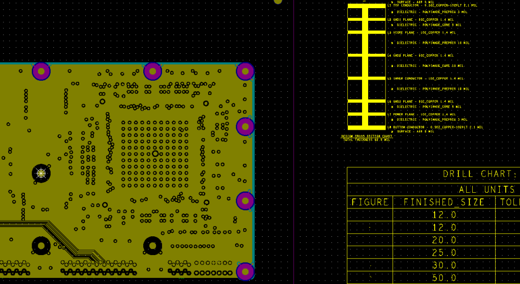
It is also worthy to know what Gerber files contain before getting into the process of verification. There will be several Gerber files in your standard PCB project, each of which corresponds to a layer or other aspect of your board. You will have copper traces, silkscreen traces, solder mask traces and all those holes will have drill files.
The best thing about checking Gerbers is that you are actually looking at what the manufacturer will actually get, not what your design package is displaying to you. At other times there is a lack of connection between the two and this is where this step comes in. Your CAD software might display things one way, but the exported Gerbers could tell a different story.
Getting Started with the Right Tools
The initial one is a good Gerber viewer. Although professional desktop applications exist, a Gerber file viewer online will present the best combination of convenience and functionality to many designers. These web-based applications allow you to transfer your files fast and view them without installing some other application. They also come in especially conveniently when you are operating on different computers or have team members that may not have the special PCB software.
When choosing a viewer, seek one that can accept RS-274X format (the current Gerber standard) and accept drill files. The capability to switch layers on and off, zoom in to have a detailed look and measure distances between the features are all indispensable features that you will use frequently.
The Layer-by-Layer Inspection Process
Begin your review by placing all your Gerber files into the viewer and have a feel of the entire picture. Start by the copper layers, the heart of your design. Check the top and bottom layers, and see whether there are any traces of unduly thin or broad. Ensure that pads are well attached and no untold copper remains are left that may lead to shortages.
Be careful of high-density routed areas or those with small components. Make sure that the distance between traces matches the capabilities of your manufacturer. A trace which appears fine when viewed at normal magnitude may be dangerously near a neighbor when viewed with greater attention. This is a time also to verify your ground planes and power pours to be sure that they have been created correctly and that they have no unexpected gaps.
Then check your drill files by overprinting them on your copper layers. Each hole of the drill should fall in the middle of its pad. Holes that do not align are a typical manufacturing nightmare which will make your board useless. It is also important to make sure that the size of holes is right and serves the intended purpose. You may also wish to check wire gauge calculator online to ensure that your through-hole component leads will easily pass through their respective holes with enough space to fit them through and allow you to properly solder them in.
The Devil’s in the Silkscreen Details
Silkscreen layer, though not electrically important, but should not be ignored. There are professional-appearing board designators and polarity markings, which are clear and readable. Ensure your silkscreen text is not so small that it is illegible, your manufacturer will normally specify minimum text size, usually between 0.15mm line width and 1mm character height.
Also check that silkscreen components are not crossing pads or falling into spaces where they will be covered by other components. Nothing is worse than falling into the trap of having your carefully designed reference designators only to find that after the board has been put together they are nowhere to be found. Ensure that diode, capacitor and connector polarity indicators are visible and in place.
Checking the Solder Mask Layer
The solder mask layer is something that should be looked at closely as it will determine the reliability of your board and the manufacturability as well. Check that the pads are well solder mask relieved, that the holes in the solder mask exposing the copper to be soldered are open. Too small pads in comparison to their solder mask holes may cause solder bridges, and insufficient clearance may cause the difficulty of soldering.
Search in places where the solder mask may be too fine and cause the solder mask to peel or damage during assembly. With a flexible PCB manufacturer this becomes all the more important as flex boards are subject to mechanical stress that may damage poorly designed solder mask.
Running the Numbers
It is always a good idea to check before submitting your Gerber that your design is within your budget expectations. Check your board size, number of layers and any special considerations such as controlled impedance, or unusual materials. Such factors play an important role in PCB fabrication cost and the sooner you notice inconsistencies the better you can avoid cost shocks in the future.
Ensure that you have properly defined your board outline and cutouts or routing information. These must be evident in your mechanical layer or board outline file. This information is required by the manufacturers to know precisely how to remove your board off the production panel.
The Final Pre-Flight Checklist
This mental checklist you should go through as you head into the finish line. Ensure that all the layers are there and correctly named, check your drill to copper clearances is within manufacturing requirements, no floating copper areas that can cause manufacturing problems, and all text and markings are of an appropriate size and location.
It is also prudent that you compare your Gerber files with your original design schematic. This may appear unnecessary, but a last sanity check may identify mistakes that may have been added during the layout process or Gerber generation.
Moving Forward with Confidence
It may be a drag to go out of your way to ensure that you completely verify your Gerber files before printing them, but it is a payoff that can be rewarded by the time saved in reliability and cost. Every minute of a close examination would save hours of troubleshooting and hundreds of dollars of remake time.